In a TEM, a broad parallel beam of electrons is sent though a thin sample and an image or a diffraction pattern is recorded from the transmitted signal. In this way, TEM analysis offers structural information of samples at the nano- or atomic scale. Specifically, the information is provided through bright- or dark-field TEM imaging, high-resolution TEM imaging, and selected area electron diffraction.
The microscopes can also be operated in STEM mode where the beam is focused into a small spot (below 1 nm). The bright- or dark-field STEM images are formed by raster scanning the beam over the sample.
In addition to the structural information, the relevant sample composition can be revealed by recording x-rays produced from electron-sample interactions (EDS) or by recording the energy loss of the transmitted electrons (EELS).
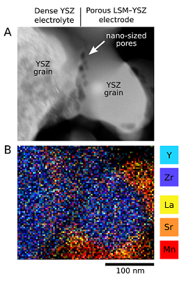
Figure: Dark-field STEM image (A) and an elemental EDS map (B) of a degraded solid oxide electrolysis cell (Nat. Mater 14 (2015) 239–244)
Equipment
- JEM3000F equipped with a 300kV FEG, a 4k CCD (Gatan MSC), a STEM unit, BF and HAADF STEM detector, a 30 mm2 EDS detector with a SATW window (Oxford Instruments) and a GIF2000 (Gatan) for EELS and EFTEM analysis.
Location: Risø Campus, B228, R105
- JEM2100 equipped with a 80-200kV LaB6 gun, a 4k CCD (TVIPS F416), a 1k fast scan CCD (TVIPS F114TR), a STEM unit, BF and HAADF STEM detector, a 30 mm2 EDS detector (JEOL JED-2300T).
Location: Risø Campus, B227, R k04-k10
- TEM holders include JEOL single tilt holders, JEOL double tilt holders, JEOL low background double tilt holders, a Gatan single tilt heating holder (max temperature 1300°C), a JEOL double tilt heating holder (max temperature 800°C), a Hysitron nanoindentation holder.
- In addition to our in-house TEM equipment DTU Energy have access to DTUs dedicated microscopy facility, DTU CEN, where for example do in situ heating experiments in reactive gas environments.
Contact
Søren Bredmose Simonsen