A scanning electron microscope (SEM) is a very versatile piece of equipment. It works by scanning a focused beam of accelerated electrons across a surface and measuring the various emitted signals using different detectors. Several different sample characteristics can be investigated depending on which detectors are utilized:
Topology and high resolution
The SEMs available at the department allows image resolutions down to approx. 1 nm under the right conditions. The SE2 detector located off to the side in the microscope chamber gives excellent topological contrast and the In-lens detector situated in the beam path provides very high detection efficiency. These two detectors (or others) can be used simultaneously to obtain an image pair with complementary sample information.
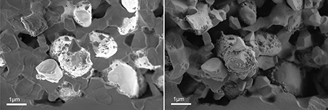
Figure 1: An In-lens (left) and SE2 (right) detector pair of the same sample location.
Compositional contrast
Compositional contrast between different elements in the sample can be studied using the backscattered electron detectors (BSE or AsB) or the energy selection backscatter detector (EsB). These detectors allow the spatial distribution of different phases to be imaged. The EsB detector in particular provides excellent compositional contrast with the ability to filter away almost all topological information.
Figure 2: An overview image showing compositional contrast of several PLD layers using the EsB detector.
Element analysis
Identification of specific elements in a sample is possible using the Energy Dispersive X-ray Spectroscopy EDS system. Based on the detection of characteristics x-rays the EDS system is able to spatially identify and map the elements in a sample.
Equipment
- Zeiss Merlin FEGSEM microscope equipped with HE-SE2, In-lens, EsB, AsB and STEM detectors, an EDS system and an EBSD system.

Location: B310, R902
- Zeiss Ultra FEGSEM microscope equipped with SE2 (Everhart-Thornley), In-lens (SE1) secondary electron detectors; four quadrant solid-state angular selective (AsB) and In-lens energy selective (EsB) backscattered electron detectors; an EDS system (Bruker X-Flash 630M).
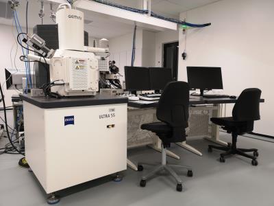
Location: B310, R901
- Zeiss Crossbeam FEGSEM microscope equipped with SE, In-lens, and BSE detectors; and an EDS system (Thermo-Fisher).
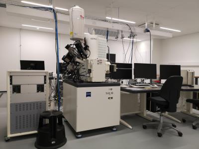
Location: B310, R901
- Zeiss EVO Tungsten Filament SEM equipped with SE and BSE detectors and an EDS system (Oxford Instruments, Q-Max (80mm2)).
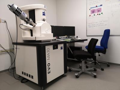
Location: B310, R121A
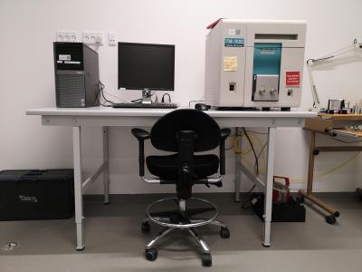
- Hitachi TM3000 Tungsten Filament tabletop microscope equipped with BSE detector and an EDS system (Bruker X-Flash).
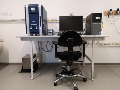
Location: B310, R121A
- Hitachi TM1000 Tungsten Filament tabletop microscope equipped with BSE detector.
Location: B310, R121A
Contact
Karl Thydén, Salvatore De Angelis